madoka82
註冊時間: 2008-09-14
文章: 2
|  發表於: 星期四 九月 25, 2008 8:29 pm 文章主題: 請教輸出變壓器的串並連的問題 發表於: 星期四 九月 25, 2008 8:29 pm 文章主題: 請教輸出變壓器的串並連的問題 |  |
| | 我目前要裝的機器算是誠文堂新光社"Audio真空管AMP製作Guide"裡頭刊載的 6BM8 超三結綜合擴大機‧相信不少前輩應該也看過相關的網頁網頁中段有電路圖。 | |
Colin網站討論區裡madoka82發表以上的問題。
我上了
相關的網頁看了。第一次聽到super Triode connection STC "超三結", 不知妙在那裡,跟super一詞有何關連?
陽光之下無新事。
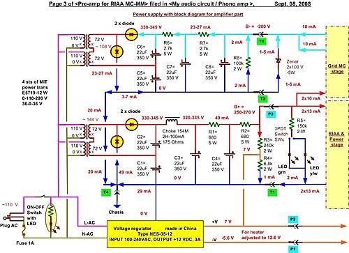
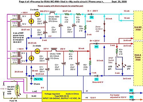
我把電路圖下載,分析一下。
圖裡藍色跟紅色字是我加上的
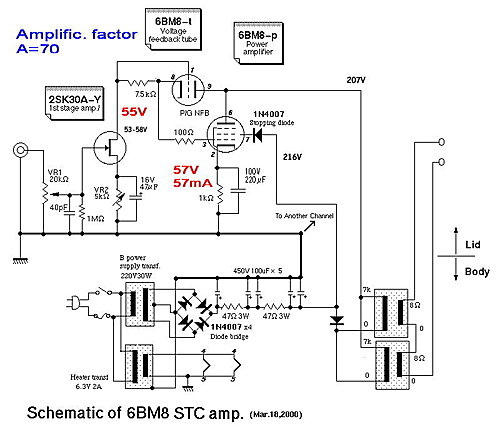
把opt 7000/8初級併聯、次級串連,相當於圈數比由 30減半為15, 負載變成1800/8 或 7000/32.
5極pentode部分是維持5極接法,不過7腳第二柵極高出6腳屏極10V(5極管的第二柵極電壓,直接影響特性)。
輸入信號電壓由2SK30A放大,它的負載是主動方式active loading由6BM8三極Triode負責。
因為陰極電阻7.5k沒有傍路電容,引起電流迴授,管內阻增加為(1+AF)*7.5k =~ 70*7.5=~ 525k,總的負載加上7.5k,高到530k。
這樣不必提高B+電壓,可以達到高負載、高線性、高輸出的效果,而且輸出由8腳陰極作隨耦cathode follower有低輸出阻抗的好處,這就是所謂的"Shunt Regulated Push-Pull (SRPP 天底下有這麼好康的嗎?)
正常的SRPP接法第9腳屏極 有獨立的B+,但這裡是跟第6腳掛在一起的,構成圖上說的NFB負迴授。
當opt─6BM8-pentode 屏流增大,9-6腳電壓降低,6BM8-Triode工作電壓下降,導致6BM8-p柵極電壓跟著下降,屏流減少。是正港的NFB.
要問的是NFB量是多少?
6BM8-Triode內阻(如前推論是530k以上) 跟7.5k構成分壓回路,迴授因素Beta=7.5k/530k=1/70.
因此6BM8加了NFB之後的電壓放大,按照公式:
A0=A/(1+A*Beta),
A*Beta遠大於1,
因此
A0=A/A*Beta=1/Beta=70
約70倍的放大率, 近於40dB的電壓增益。
opt 1800/8, N=15, 減為 15
70/15=4.7倍, 整體增壓倍數 還要看第一段的2SK30A放大倍數是多少了。
一般power amplifier整體應該十位數,或50倍就很夠了。
等同的2SK30A放大倍數10就夠了。
結論是:
看不出妙在何處?
像我的"3支全壘打",直接交連─3極接法已經滿意了。
 剛剛進入Katsu-San用英文說明的,簡單明瞭。
STC整體來看,放大倍數,如我推論的等於6BM8-t的amplification factor A(Katsu-San文中mu) 70, 內阻約是cathode follower =1/gm=1xxR,近似於把6BM8 五極管pentode轉換成三極管Triode的性能。
我猜想這是名稱Super的由來。
構成要件是:
輸入段要是current source signal
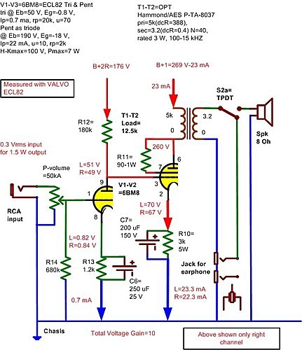
http://www.gem.hi-ho.ne.jp/katsu-san/audio/what_STC1_english.htmlThe Super Triode Connection Ver.1
- For the transistor generation -
The Super Triode Connection (STC), invented by Shinichi Kamijo, uses triode as feedback path device instead of a resistor as conventionally. By this method the STC adopts the triode's performance characteristics, so you get the sonic of the triode used with a low plate resistor, even if you actually are employing a pentode, beam deflection tetrode or even a transistor, as power output (current amplification) device.
Kamijo-san's home page is here.
Shinichi Kamijo invented several types of STC, but here I focus on the Version 1 type, because it exemplifies the basic idea underlying all STC types. I think you can readily understand the others if you understand the Ver.1 topology.
In addition, probably you may feel the STC-MX (my original idea) is complicated, but if you can understand the Ver.1 basics, then you may find it is not actually very difficult.
However, understanding the STC topology may not be so easy for the younger generation, because young people versed in semiconductor based technology do not properly know how tubes and tube circuitry work. I believe one of the biggest problems is the triode itself, because it is a voltage output device, whereas the transistor is a current output device.
Furthermore, the STC uses the triode as a feedback path device. This is a very unusual way to use a triode. Therefore, here I explain the STC from the point of view of people who understand transistors.
The figure below shows the basic schematic of an STC amplifier, and that at below-right is the equivalent circuit. In this circuit, probably those of the transistor age cannot easily understand this "triode feedback".
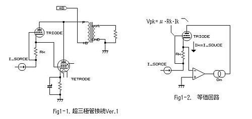
Figure 1; Basic STC Schematic, and Equivalent Circuit I will not explain the tetrode or pentode function here, because these devices have similar characteristics to comparable semiconductor devices (e.g. depletion mode FET's). In short, it is enough if you can understand that they are current output devices.
First of all, in order to understand the STC, you need to know how a triode actually works. If you are familiar with transistors, suspect that you are used to thinking about the device working in terms of current. But here you have to think about it in terms of voltage instead of current.
There is a 'heater' inside of the cathode, and it heats red-hot. The heater heats the cathode to cause it to emit electrons. Electrons are energized by the heat resulting in this emission effect. Therefore, in order to increase those electrons - in other words to increase the current - heater needs to spend much more power.
As you know, an electron has a minus electrical charge, so electrons will be attracted if there is plus charge in proximity. This is the role of the plate of the triode tube. As a result, "electron current" flows from cathode to plate. (But "conventional current" flows from positive to negative, so the resultant tube (conventional) current is described as flowing from plate to cathode).
The GRID can be used to control this current flow. To do so, the grid potential is set-up (「biased」) such as to be negative with respect to the cathode. The plate is set up with a high positive voltage potential, so the negatively charged electrons emitted from the cathode, go to the plate, but are interrupted by the effect of the voltage at the grid. Therefore, the (conventional) current flow from plate to cathode is controllable by the grid.
The grid is at no particular voltage level at all, until external resistors or voltage references are connected to the grid and to the cathode. The grid must be "biased" by these means, to properly enable control of the cathode-plate current. Free of any control by the grid, the tube is naturally conducting very significantly. Most bias arrangements therefore always act to "back off" this natural cathode-plate current flow; the grid is thus almost always operated ("biased") with negative voltages, with respect to the cathode. The tube is like a JFET in this regard, and not like a MOSFET or bipolar transistor at all, where "bias" is typically "forward" and involving positive control element voltages.
Negative voltages at the grid, which is physically in close proximity to the cathode, inhibit the emission of electrons, being also negatively charged, from the cathode. The more negative the grid, the more electron flow from cathode to plate is inhibited, the less current flows. The less negative the grid, the more cathode-plate (electron) current can flow.
The grid must be "biased" by either;
(a) "fixed bias" = application of external minus DC supply to the grid, with cathode grounded, or
(b) "cathode bias" (also called "self bias") = cathode caused to be positive relative to the grid (that is to say "grid minus relative to cathode" again), by adding a resistor in series with the cathode (to ground). The natural flow of plate-cathode current in the tube itself creates the bias voltage. It is also necessary to return the grid to ground via a (typically very high value) resistor, for this bias to work. The STC Ver.1 uses method (a) for bias for the feedback triode*, and output tetrode/pentode is method (b). But in the case of the feedback triode, controlling current through the feedback triode's cathode resistor (Rk in Figure 1) not only sets up static bias, but is also the means for applying audio signal drive too.
(*Note: Please be care, the topology of feed-back triode is similar to self-bias, but the bias voltage is clearly "fixed" if no audio signal. "Fixed bias " does not mean the topology, but the "method" to decide the bias voltage.)
Therefore, the current flow from plate to cathode is controlled by the grid.
At the same time, if the plate voltage potential is deliberately raised, the electrons from the cathode will be attracted more strongly, and the current flow is increased. So, as a result, both the plate to cathode voltage (Vpk) and the grid to cathode voltage (Vgk) can change (control) the current flow. So the plate to cathode current Ik(=plate current Ip) increases or decreases in proportion to the Vpk and the Vgk;
Ip = C0·Vpk, and Ip = C1·Vgk : Here C0 and C1 are proportional constant.
The proportional constant C
0 is usually referred to by its inverse function conventionally, which is termed 'rp' (plate resistance);
Ip = (1/rp)·Vpk = Vpk/rp
And the proportional constant C
1 is termed 'gm' ("transconductance");
Ip = gm·Vgk
Please remember these relationships.
With the plate directly connected to some positive voltage, one must imagine that there is this imaginary internal plate resistor 'rp' between that positive voltage and the plate. This is quite different behaviour to pentode, tetrode and indeed transistor behaviour.
It means that the plate voltage Vpk will change if the "infinite load" is connected to plate or cathode, because Vgk changes the plate current Ip, and the voltage is defined by the internal resistance 'rp' .
Vpk = C2.Vgk
So now the plate to cathode voltage is also controlled by Vgk, not just the plate current Ip. The proportional constant between Vgk and Vpk (C
2) is called 'mu'.
Vpk = mu·Vgk
Or, put another way;
mu = Vpk/Vgk
Now all these equations shown above may be simply combined;
Ip = Vpk/rp = gm·Vgk
Rearranging a little, gives the basic equation describing the performance of a triode;
Vpk/Vgk = gm·rp = mu (a constant)
An implication of this is that when current Ip passes through the internal plate resistance rp, some voltage will be dropped by that rp. For most other active devices (pentodes, transistors) this internal or "source" resistance is considered almost infinitely high, and changes in Ip (or its equivalent) produce hardly any such internal changes in voltage at the plate (or collector) etc. That is to say, these other devices have an internal plate/collector characteristic like a "current source".
In the case of the triode however, if rp were low enough, the output characteristics of the plate will be akin to a voltage source rather than a current source. This is the biggest difference between semiconductor.
In conclusion, let us restate and summarize the equations of the triode;
- The voltage Vpk changes according to Ip if passing through rp, so;
Ip·rp = Vpk.
- mu is the proportional constant between Vgk and Vpk, so;
Vpk = mu·Vgk.
- gm is the proportional constant between Ip and Vgk, so;
Ip = Vgk·gm.
- Therefore, mu = rp·gm.
Please consider now the graph shown below. This is called the 'plate characteristic' diagram, as it shows the relationship between Ip and Vpk and Vgk. (Note that this particular diagram is idealized; it shows the characteristic of an ideal triode, not necessarily a real-world one!)
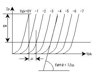 Figure 2. Triode characteristics
 Here you can find many slanting lines, each reflecting a different value of Vgk. The horizontal axis is Vpk and vertical axis is Ip.
You can easily to understand that Vgk will control the plate voltage Vpk, but note that each of the three parameters shown will affect the others. This graph shows these basic relationships.
The parameters mu, rp and gm may be derived from these curves.
• rp = Vpk/Ip is the inverse of the slope of the Vgk lines. So rp is the tangent ratio of the angle (theta) shown on the diagram.
• Gm = Ip/Vgk, so is shown as the change on the vertical (Ip) axis (marked in the diagram) per unit change in Vgk (the change from Vgk = -1V to Vgk = 0V as shown).
• mu = Vpk/Vgk, so is the change in Vpk on the horizontal axis per unit change in Vgk (shown as the change from Vgk = -1V to Vgk = -2V on the diagram).
Now let us consider the operating conditions, specifically the load line, for the feedback triode (not the overall amplifier). Maybe you have previously learned that the angle of the load line gives the resistance value of the load. But this is not always so. The load line of the feedback triode is not defined by a load resistance, but by a "current source signal".
Firstly, I will explain the "current source signal".
To start with, recall that a VOLTAGE source signal, which perhaps you are more familiar with seeing, has (in theory at least) zero source impedance. This says that the source voltage follows the audio signal absolutely, independently of the load. High impedance load, or low impedance load, the signal source supplies however much current is demanded. And (again "in theory"), the audio signal voltage is never changed by such loading.
That is a "voltage source signal". A "current source signal" is just the opposite!
A CURRENT source signal has infinite source impedance ("in theory"). This says that the source current follows the audio signal absolutely, independently of the load. High impedance load, or low impedance load, the signal source supplies whatever voltage level is demanded such as to drive that current. The audio signal current is never changed by such loading.
An alternate way to look at the "current source signal" is to imagine the more familiar "CCS" or "Constant Current Source". This outputs a constant current, independent of the load circuit it feeds. But then imagine that the actual value of CCS current is not absolutely fixed, but is able to be modulated. Now let the audio signal be the CCS current value "control signal".
In the STC Ver. 1, the cathode of the feedback triode is connected to a "current source signal". The current source signal has near-infinite source impedance value. So the current flow through the feedback triode will be determined solely by this current source value. In this case, the current through the feedback triode is "independent" of the internal plate resistance, rp.
Another outcome of the current source signal having effectively an infinite internal (source) impedance, is the feedback triode's plate-cathode current flowing at a constant level (albeit with modulation due to the audio signal). This means that whatever voltage potential appears at its cathode depends (using Ohm's Law) on;
(a) the current source signal μA or mA value, moment by moment, and
(b) the load resistance connected to it. Whether a low resistance or a high resistance, even a "Meg-Ohm" resistor, the voltage at the current source output is always just (a) x (b).
The (effective or dynamic) source impedance of a practical current source signal can be expected to be, and treated as, effectively infinite in value.
To recap then, the "current source signal" means that the current source's actual μA or mA value is modulated by the audio input signal. This is the equivalent action of a pentode, tetrode (or FET) as the input device, because if you connect the grid of a pentode or tetrode to the input signal voltage, then the plate current will be modulated by that signal voltage, (the plate being treated as having near-infinite source impedance).
Let's now think about the load line of the STC and its actual manner of operation here. The most important feature is the feedback triode. It is connected between the plate and the cathode of the output tetrode/pentode tube. This triode provides the 'feedback path' for the output tube's plate to grid negative feedback(NFB). I will explain how it works in this feedback mode, shortly.
Given that you now already understand how the triode actually works, I'll explain the feedback triode of the STC with the aid of the example shown below.
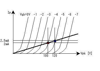 Figure 3; load line
Initially, let the plate current of the triode be 2mA, with Vgk is -4V, meaning that Vpk is 100V. This is indicated by the left-hand point (red) on this Figure.
Look now again at the equivalent circuit shown in Figure 1. In Figure 1, Ik = I(Rk) = I_source.
Basically, the grid of a tube has a very high input impedance, so the grid current(s) can be safely neglected, and so Ip =Ik. This Ik is the Ip in Figure 3.
Now we can be sure that Vgk will be zero if the Ip is zero, since no Ik means no voltage developed across Rk. So the load-line for the feedback triode has to pass through the origin (zero-zero point on the graph).
Vpk = Ip·Rk, so the Rk has to be 2kohms, i.e. 4V ( as Vgk) divided by 2mA (as Ip = Ik).
Let now the Ip increase to 2.5mA, (say due to the input signal drive). Let's initially assume the plate potential stays the same. But Vgk will change; the value of Vgk must become 2kohm x 2.5mA = -5V.
This is indicated as the right-hand point (blue) in Figure 3. Now from this diagram, Vpk has to now be 120V, if Ip is 2.5mA and Vgk is -5V.
But the plate potential (relative to chassis ground, 0V) was defined as "unchanged", so instead the cathode potential must change; the cathode potential must drop. (It is impossible to change the plate voltage by the small feedback-triode current, because the load resistance is too small for that current.)
Now the cathode of feedback triode is connected to the grid of output tube and the current signal source, so the grid of output tube potential is unsettled. By changing feedback triode cathode potential, Vpk will be 120V.
Basically, the output current Ip of the output tetrode/pentode is determined only by its Vgk. Since this grid bias on the output tube will become more negative, less plate current Ip will flow in it. It's Its plate voltage will tend to rise. Vp (the plate voltage relative to chassis ground, 0V) of the output tetrode/pentode will rise toward 120V.
Now look at Figure 1 again.
The output current of this amplifier is only defined by the triode Vpk, the feedback voltage, because the grid voltage of the output tetrode/pentode is not fixed, but floating, since the input signal 'I_source' is a current (not a voltage).
For this reason, only the feedback voltage determines the grid voltage of output tetrode.
This character is called 100% voltage feedback, because the input impedance (the source impedance of a CCS) is infinite, while the feedback resistor has some defined, real value, being the rp of the feedback triode.
This operation is similar to that of a high gain operational amplifier.
OK, now let's get back to the load-line. The load-line passes through both the points marked and zero-zero on Figure 3. This is the load-line for the feedback triode, but not the complete amplifier.
The input signal of the amplifier is a current, not a voltage. We can say that the output voltage will be changed by the input signal current working the feedback triode along its load-line.
I write that the output voltage will be changed, but of course the feedback is not superconductivity(!), so the output has some output impedance.
The value of output impedance is determined by the characteristic of output tetrode.
As I already explained, this is 100% voltage feedback, so it is defined by the trans-conductance (gm) of output tetrode, because it defines the open voltage gain.
Ip of tetrode/pentode is determined by Vgk and proportional constant 'gm' (transconductance);
Ip=gm·Vgk, so Vgk=Ip/gm
So, if the load resitance(or impedance) is RL, the open loop voltage of tetrode;
Vout=RL·Ip
gain of tetrode Av is Vout/Vin. From above two equations;
Av=gm·RL
And thus, the output impedance Ro is determined by 100% feedback,
Ro=RL/(gm·RL) = 1/gm
this is just the same as cathode follower.
If the gm of the output tube is higher, then the open-loop gain, gm.RL as above, will higher. The feedback will therefore also be increased (as there is 100% voltage feedback), and so the output impedance becomes lower.
Now, we can look at the characteristic of whole STC amplifier. As I already explained, an output impedance is the angle of plate characteristics lines, and it is the proportional constant of Vpk and Ip.
I previously explained how, for a triode, source or output impedance rp is given by Vpk/Ip which is the inverse of the slope of the Vgk lines seen in Figure 2; rp is the 1/tan of the angle (theta) shown on the Figure 2 diagram.
The characteristic of the whole amplifier may be considered in a similar, parallel way. Instead of "rp" for the triode, instead consider "Ro" (and Ro = 1/gm) for the characteristic of the complete amplifier.
Therefore, the characteristic of whole amplifier can be approximated by the slanting linear lines, the angle of the line is 1/gm. The amplitude factor has to be the same as feedback triode, so it has to be mu, but this is not real amplitude factor but the current to voltage conversion factor.
The below graph is the load line of RL and characteristics of whole amplifier. Please notice, slanting lines are not defined by the input voltage, but by the input current (Ik). This is the characteristic of STC Ver.1.
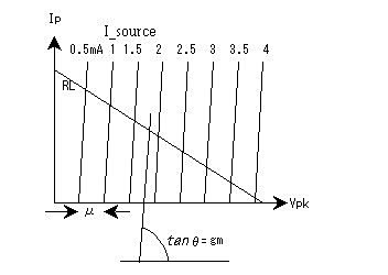
Figure 4: Overall characteristics of the STC Ver. 1
Of course, you have to define the RL from the raw characteristics of output tetrode/pentode. Generally speaking, this character is further constrained and defined by the knee point, maximum current and maximum plate dissipation of the output pentode.
As the feedback is not the magic, the original characteristics of the output tetrode/pentode are not changed by the feedback.
The STC amplifier overall characteristic is achieved by controlling the grid voltage of the output tube such as to take on the characteristics of the feedback triode.
In other words, Vpk of the feedback triode is defined by its mu, so the grid voltage of the output tetrode/pentode is controlled to achieve the same character automatically.
The last step is that we have to define the input current, I_source = Ik. If you are familiar with semiconductors and their theory of operation, then this is easy to do.
For instance, if you use a transistor for the input device, you can determine an appropriate emitter resistor from knowing the maximum input voltage.
The output (collector) current of this transistor will be defined by that emitter resistor.
This is the simplest method, but is typically sufficient.
Abstract in English
Home (Japanese)
* Special thanks; Paul.
Last update 5th/Nov./2002